You are here:

ONFI 3.2 NAND Flash Controller
The ONFI 3.0 NAND Flash Controller IP Core supports the Open NAND Flash Interface Working Group (ONFI) 3.0 standard and is backwards compatible. It uses differential signaling on the clock and data lines and clocks at any frequency up to 200 MHz.
The ONFI 3.0 NAND Flash Controller is a full featured, easy to use, synthesizable design that is easily integrated into any SoC or FPGA development. Designed to support both SLC and MLC flash memories, it is flexible in use and easy in implementation. The controller works with any suitable memory device up to 128 Gb from leading memory providers such as Micron, Samsung, Toshiba, Hynix, ST-Micro, and others.
The IP core includes a host of configuration options from page size to band selects. The controller offers Hamming Code (1bit error correction and 2bit error detection) and BCH (option for 4-, 8-, 12-, up to 64 bit error correction) error code correction (ECC) for optimized performance and reliability. Additional features include the capability to boot from flash.
The controller supports a variety of host bus interfaces for easy adoption into any design architecture. An optional NAND Flash file system is available to support advanced features. The file system converts complicated tasks of NAND flash memory interfacing to simple memory accesses. Flash memory read, write, garbage collection, bad block management, and other functions are handled by the file system in the background.
The cores are delivered in Verilog RTL that can be implemented in an ASIC or FPGA. They are fully tested with vendor models and hardware tested with FPGA-based HDK products. The core includes RTL code, test scripts and a test environment for complete simulation and verification.
查看 ONFI 3.2 NAND Flash Controller 详细介绍:
- 查看 ONFI 3.2 NAND Flash Controller 完整数据手册
- 联系 ONFI 3.2 NAND Flash Controller 供应商
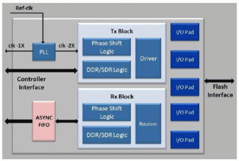
Block Diagram of the ONFI 3.2 NAND Flash Controller

ONFI 3.2 NAND Flash Controller IP
- ONFI 4.1 NAND Flash Controller & PHY & IO Pads on 16nm
- ONFI 3.2 NV-DDR2 PHY in GDSII
- ONFI 4.1 NAND Flash Controller & PHY & IO Pads on 12nm
- ONFI 4.1 NAND Flash Controller & PHY & IO Pads on 28nm
- ONFI 4.1 PHY IP (Silicon Proven in TSMC 12FFC)
- ONFi PHY 4.0 (FPHY+MDLL+SDLL Regulator) (Silicon Proven in TSMC 28HPC+)


