


You are here:
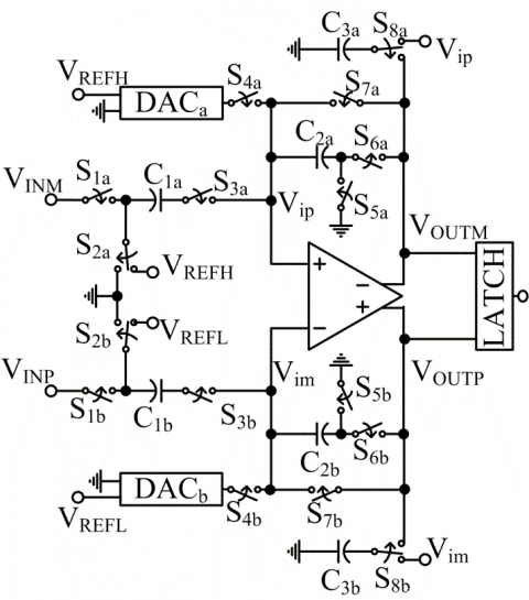
Low power 9 bit cyclic ADC
The ADC is a fully differential 9-bit cyclic ADC which utilizes 4-bit binary weighted array to obtain 9-bit resolution. Cyclic algorithm for the ADC conversion is used to reduce number of capacitors in the capacitor array and save layout area. The ADC is designed for suppression of the supply variation, even in the conversion cycle.
查看 Low power 9 bit cyclic ADC 详细介绍:
- 查看 Low power 9 bit cyclic ADC 完整数据手册
- 联系 Low power 9 bit cyclic ADC 供应商
Block Diagram of the Low power 9 bit cyclic ADC
