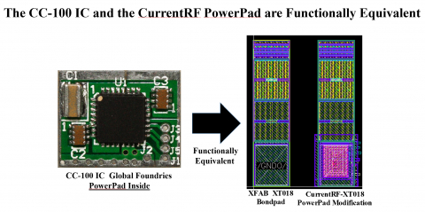
Power and Ground BondPads
Adding on-chip supply bypass capacitors provide a local high frequency current reservoir for local logic, reducing supply EM noise by bypassing the digitally generated, high frequency noise currents to system ground. This capacitor bypassing action, however, shunts the high frequency EM surges and noise currents away from the supply line ultimately causing a “throw away” DC power drain (i.e. DC recharging of the bypass capacitors due to the losses and overlap currents in the system) supplied by system power sources, batteries, and capacitors.
Power draw due to these digitally derived noise currents and losses can be greater than 50% of the total device and system power consumption. They are especially significant in battery operated systems and portable devices, such as smart phones, portable computing devices, laptops and iPads, medical devices, ultra-low power systems powered by low capacity energy harvesting devices, and the like. This form of digital power drain tends to increase system size weight and Power (SWaP) as the consuming device is utilized more heavily and application complexity increases in digitally driven systems.
To reduce the above mentioned EM power drain, the conventional design wisdom is to use digital strategies in design so as to periodically deactivate power hungry digital circuits (some form of “burst mode” processing), reduce system clock rates, minimize digital supply voltages, or “process shrink” the design to a lower gate length manufacturing process node. The strategies above can be thought of as power saving “defensive” actions, the designer striving to reduce switching circuit power drain as much as possible. Utilizing the above strategies generally requires some form of design rework on the digital circuits in order to accomplish the desired power reduction, which adds to time to market and cost. It should be noted, that no matter what “defensive” choices designers make in attempting to reduce digital EM power drain, a certain magnitude of “thrown away” current and power always remains when switching circuits are active. So long as designers use electron-based transistor devices in design, this type of energy waste will be present. This form of power drain can be thought of as a previously “forgotten” EM energy source embedded in switching systems, considered unreachable and unusable, until now.
Maintaining the Fit, Form, and Function of conventional Supply Line Bondpads, the CurrentRF PowerPad Supply Line Bondpad reduces the overlap current digital power drain, tapping into this capacitor bypassed source of wasted power, recycling and reducing 20% to 40% of the total Digital Power Draw. Targeting digital “thrown away” currents, the PowerPad Supply Line Bondpad intercepts and recycles these currents back into a given IC power grid, reducing overall Digital Power Draw. The implementation of the CurrentRF Powerpad Supply Line Bondpad is small and inexpensive enough to be integrated into the padring of any Digital or Mixed Signal IC, and/or into existing and new IC bondpads, drawing no operational power of it’s own.
The CurrentRF Powerpad is currently available on TSMC and XFAB process nodes, and customizable for any modern foundry process.
查看 Power and Ground BondPads that include CC-100IP Digital and Switching Circuit Power Reduction Technology, Featuring 20% to 40% Total Dynamic Power Reduction 详细介绍:
- 查看 Power and Ground BondPads that include CC-100IP Digital and Switching Circuit Power Reduction Technology, Featuring 20% to 40% Total Dynamic Power Reduction 完整数据手册
- 联系 Power and Ground BondPads that include CC-100IP Digital and Switching Circuit Power Reduction Technology, Featuring 20% to 40% Total Dynamic Power Reduction 供应商
Block Diagram of the Power and Ground BondPads that include CC-100IP Digital and Switching Circuit Power Reduction Technology, Featuring 20% to 40% Total Dynamic Power Reduction

Video Demo of the Power and Ground BondPads that include CC-100IP Digital and Switching Circuit Power Reduction Technology, Featuring 20% to 40% Total Dynamic Power Reduction
The CurrentRF PowerPad embedded in a demonstration PowerStic Module


