PCI Express Gen 1/Gen 2 Phy
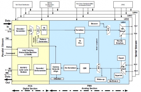
Each transmit section of the TRC5024CPA contains a low-jitter clock synthesizer, a parallel to serial converter with built in PCS transmit functions, and a CMOS output driver with selectable de-emphasis for use in backplane applications.
Each receive section contains an input limiting amplifier with on-chip terminations and selectable equalization levels, clock/data recovery PLL, and PCS receive functions. Built-in serial and parallel loopback modes. PRBS generator/checker and error detectors aid in support of testing.
The TRC5024CPA requires no external components for its clock synthesizers and clock recovery PLL. Three external resistors are needed to set the proper bias currents for its onchip terminations.
TRC5024CPA has low jitter generation and high jitter tolerance making it ideal for integration in SoCs and ASICs in the presence of multiple clocks and noise. TSMC is available in TSMC 65 nm G process and can be ported to other processes.
查看 PCI Express Gen 1/Gen 2 Phy 详细介绍:
- 查看 PCI Express Gen 1/Gen 2 Phy 完整数据手册
- 联系 PCI Express Gen 1/Gen 2 Phy 供应商
Block Diagram of the PCI Express Gen 1/Gen 2 Phy

PCI Express Phy IP
- PCIe 7.0 PHY IP supporting the latest features of the evolving PCIe 7.0 specification to enable 128 GT/s and up to x16 lane configurations
- PCIe 5.0 Serdes PHY IP, Silicon Proven in TSMC 12FFC
- PCI Express PHY serial link PIPE Transceiver IP cell/hard macro
- PCI Express GEN-3/Display Port SERDES PHY - Samsung 28 28LPP
- PCI Express GEN-3/SATA3 SERDES PHY - Samsung 28 28FDSOI
- PCI Express GEN 3/4 Port SERDES PHY - Samsung 14LPP


