TSMC GF Intel Low Phase Noise, High-performance Digital LC PLL


You are here:
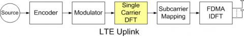
LTE Single Carrier FFT Circuit
Centar's DFT circuit can perform all 35 transform sizes needed to implement the LTE SC-FDMA protocols. It is x3 faster than the Altera equivalent and the Xilinx version uses 68% more registers and 32% more LUTs, while the Centar circuit provides 41% higher throughput. So the overall combined gain is significant.
A number of unique architectural characteristics allow this programmable circuit to provide simultaneously high throughput, high SNQR, low power, and minimal use of LUTs and registers in an FPGA fabric. Programmability is derived from a new type of memory-based array implementation that avoids addressing conflicts. The number of cycles per DFT is reduced as a result of a novel matrix oriented algorithmic approach. Clock speeds are high (~400MHz for 65nm technology) because all computations are "localized", leading to reduced interconnect delays that are less than the logic cell delays. Short critical path lengths also lower power dissipation. Minimal numbers of LUT/registers are needed because the adaptive floating-point scaling scheme keeps word lengths much shorter than traditional fixed-scaling and block-floating point schemes. Altogether these features result in extremely efficient implementations.
A number of unique architectural characteristics allow this programmable circuit to provide simultaneously high throughput, high SNQR, low power, and minimal use of LUTs and registers in an FPGA fabric. Programmability is derived from a new type of memory-based array implementation that avoids addressing conflicts. The number of cycles per DFT is reduced as a result of a novel matrix oriented algorithmic approach. Clock speeds are high (~400MHz for 65nm technology) because all computations are "localized", leading to reduced interconnect delays that are less than the logic cell delays. Short critical path lengths also lower power dissipation. Minimal numbers of LUT/registers are needed because the adaptive floating-point scaling scheme keeps word lengths much shorter than traditional fixed-scaling and block-floating point schemes. Altogether these features result in extremely efficient implementations.
查看 LTE Single Carrier FFT Circuit 详细介绍:
- 查看 LTE Single Carrier FFT Circuit 完整数据手册
- 联系 LTE Single Carrier FFT Circuit 供应商
Block Diagram of the LTE Single Carrier FFT Circuit
