You are here:

HBM3 PHY IP at 7nm
OPENEDGES, the memory system IP provider, including DDR memory controller, DDR PHY, on-chip interconnect, and NPU IP together as an integrated solution or independent IP. They are tightly combined to bring synergy for high performance and low latency. OPENEDGES' integrated IP solutions are market and silicon-proven, featuring advanced architectures and proprietary technologies that enable customers to shorten their design and verification processes.
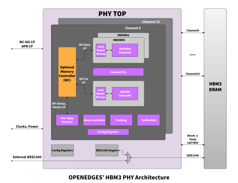
The HBM3 OPHY utilizes state-of-the-art architecture in full custom analog mixed-signal design to overcome the problem of long-term impedance drift and clock phase drift, allowing impedance and clock phase updates without the need to interrupt data traffic. The programmable timing PHY boundary combines flexibility with analog precision, and the result is ultra low PHY read/write latency between OMC and the HBM3 DRAM without sacrificing performance.
At the system level, the HBM3 OPHY was designed with minimal package substrate layer and PCB layer count in mind. This enables the integration of a HBM3 memory sub-system solution in cost sensitive applications, such as consumer edge devices, AI, GPU, HPC, STB, SSD controllers, and application processors.
查看 HBM3 PHY IP at 7nm 详细介绍:
- 查看 HBM3 PHY IP at 7nm 完整数据手册
- 联系 HBM3 PHY IP at 7nm 供应商
Block Diagram of the HBM3 PHY IP at 7nm


