High Capacity Post-Quantum Cryptography Processor (PQF-HW-LAT)
FPGA Lock IP
When triggered the core reads the ATSHA204a unique ID then generates a random 256 bit ‘challenge’ and sends this to the device. The IC performs an SHA256
hash on the challenge, a 256 bit secret key that has been programmed into it and its unique ID. The result of this hash is then returned to the FPGA Lock core.
The core then internally performs the same SHA256 hash with the challenge, secret key (which it knows) and the device ID.
If the hash result returned from the ATSHA204a matches the values calculated by the core, then an ATSHA204a programmed with the correct secret key is present
and full FPGA functionality is enabled. If not then FPGA functionality is disabled.
Counterfeit protection is provided by providing a CEM with the correct number of pre-programmed devices. Alternatively an FPGA could delay the ‘check’ trigger to allow full
manufacturing test to be performed before functionality is disabled (the internal ‘Enable’ defaults to ‘1’ at power on). When assembled boards are received from the CEM
the on board ATSHA204a devices are programmed (with the Key Write core) to permanently enable full functionality.
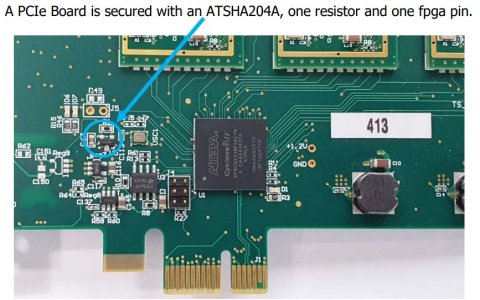
The FPGA Lockcore has a small logic footprint (~720 registers) and only uses one FPGA pin for communication with the ATSHA204A. Communication is via a bidirectional
‘open drain’ link to the device that just requires a pull up to VCC IO.
The entire hardware implementation is the SOT23-3 ATSHA204a, a pull up resistor on the interface and capacitor across the ATSHA204a power pins if required.
The Core is provided in clear VHDL so customers have complete functional visibility, a simple VHDL testbench is provided, this illustrates two consecutive HASH tests.
An accompanying Key Writer core is provided separately to allow users to program their custom secret keys into the ATSHA204A device in assembled boards.
An FPGA image with the Key Writer will program the device in a fraction of a second when programmed into the FPGA.
Example designs targeted at the Cyclone10 LP Evaluation Kit and the Digilent ‘ARTY’ Artix 7 evaluation boards are provided.
The cores use generic Intel altsyncram and Xilinx 7 series Blockram macros so should be easily built into almost any Intel FPGA or Xilinx 7 series FPGA.
These example designs include the FPGA Lock and Key Writer cores, this allows a device to be programmed then an FPGA Lock test performed to verify the key has been programmed correctly.
查看 FPGA Lock IP 详细介绍:
- 查看 FPGA Lock IP 完整数据手册
- 联系 FPGA Lock IP 供应商
Block Diagram of the FPGA Lock IP

Video Demo of the FPGA Lock IP
A quick demonstration of the FPGA_Lock and Key_Writer functionality on a CYC1000 board.
In the video where I flip the lid on the socket it removes the pressure on the socket contacts and is enough to break the contact with the data pin on the ATSHA204A.
