You are here:

CSIX to PI40
As stated by the CSIX Forum, the CSIX standard defines the physical and message layers of the interconnect between traffic managers (TM) and the switching fabric. The CSIX interface is designed to support a wide variety of system architectures and markets; and provides a framework with a common set of mechanisms for enabling a fabric and a TM to communicate. This includes unicast addressing for up to 4,096 fabric ports, and multiple traffic classes that isolate data going to the same fabric port. Link level flow control is in-band and broken into data and control queues to isolate traffic based on this granular type. Flow control between the fabric and TM is defined and is relative to both fabric port and class. Three multicast approaches are defined. The interface assumes cell segmentation in the TM, but allows compression of the transfer.
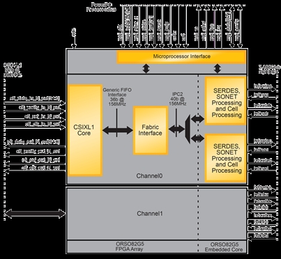
Lattice Semiconductor’s CSIX-to-PI40 core links a compliant CSIX-L1 interface to Lattice’s dual SERDES interface (compatible with PI40 interface). Inbound data frames from the CSIX port are deposited into the core's inbound FIFO. These CSIX frames are converted to PI40 cells and driven onto the dual SERDES interface. PI40 cells received on the dual SERDES interface are converted to CSIX frames and placed in the outbound FIFO. CSIX frames stored in the core's out-bound FIFOs are driven onto the outbound CSIX interface.
Lattice Semiconductor’s CSIX-to-PI40 core links a compliant CSIX-L1 interface to Lattice’s dual SERDES interface (compatible with PI40 interface). Inbound data frames from the CSIX port are deposited into the core's inbound FIFO. These CSIX frames are converted to PI40 cells and driven onto the dual SERDES interface. PI40 cells received on the dual SERDES interface are converted to CSIX frames and placed in the outbound FIFO. CSIX frames stored in the core's out-bound FIFOs are driven onto the outbound CSIX interface.
查看 CSIX to PI40 详细介绍:
- 查看 CSIX to PI40 完整数据手册
- 联系 CSIX to PI40 供应商
Block Diagram of the CSIX to PI40

FPGA IP
- RT-630-FPGA Hardware Root of Trust Security Processor for Cloud/AI/ML SoC FIPS-140
- Complete USB Type-C Power Delivery PHY, RTL, and Software
- Ethernet TSN Switch IP Core - Efficient and Massively Customizable
- CXL 2.0 Agilex FPGA Acclerator Card
- PCIe Gen3 to SRIO Gen3 Bridge (FPGA)
- 65nm/40nm Low Power eFPGA IP and Open Source FPGA Software


