H.264 High Profiles Encoder - High 10, High 4:2:2 and High 4:4:4 (12 bit 4:2:2 or 4:2:0) Profiles
You are here:

10Gbps Multi-Protocol PHY IP
Silicon-proven PHY for PCIe, USB, Ethernet, DisplayPort, and other protocols
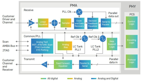
The PHY IP is designed to deliver high eye-margin at low power for backplane application. Numerous auto-calibrated circuits, programmable state machines throughout the design for PHY performance tuning, and the LC tank PLL provide low-power optimum performance.
The PHY IP is designed to deliver high eye-margin at low power for backplane application. Numerous auto-calibrated circuits, programmable state machines throughout the design for PHY performance tuning, and the LC tank PLL provide low-power optimum performance.
查看 10Gbps Multi-Protocol PHY IP 详细介绍:
- 查看 10Gbps Multi-Protocol PHY IP 完整数据手册
- 联系 10Gbps Multi-Protocol PHY IP 供应商
Block Diagram of the 10Gbps Multi-Protocol PHY IP

Multi-protocol IP
- Multi-Protocol Crypto Packet Engine, Low Power, Bus Attached
- Multi-Protocol Crypto Engine
- Multi-Protocol Crypto Engine with Classification
- Multi-Protocol Engine with Classifier, Look-Aside, 5-10 Gbps
- Multi-protocol SerDes PMA - PCIe1 PCIe2 PCIe3 PCIe4 PCIe5 and more
- 1-56/112G Multi-protocol Serdes (Interlaken, JESD204, CPRI, Ethernet, OIF/CEI)


